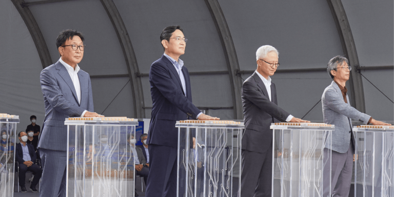
On August 19, Samsung laid the foundation stone for its future R&D center to be built on its campus in Giheung, south of Seoul. The company plans to invest $15 million by 2028 in the 109,000 square meter facility, which will be dedicated to memory chips and semiconductors, in order to overcome the limitations of scaling and consolidate its competitive advantage in electronic component technology.
Samsung is investing heavily in R&D, and on May 24 unveiled a new €330 billion investment plan to accelerate its investments in AI, biotechnology, semiconductor design and chip foundry over the next five years. When announcing this plan, Samsung said that 80% of this amount will be invested in R&D in South Korea.
Its logic chip and foundry unit recorded its highest quarterly revenue at the end of 2021 thanks to strong demand due to the global semiconductor shortage. Samsung Electronics passed its competitor INTEL and became the leader in semiconductor sales. For the foundry business, according to a TrendForce study, Samsung controls 18.3% of the market and is significantly outperformed by Taiwanese global market leader TSMC (Taiwan Semiconductor Manufacturing Company) which held 52.1% of the global foundry market in the last quarter of 2021.
Strengthening its position in the semiconductor market
The group has five semiconductor manufacturing campuses in Korea – Hwaseong, Giheung, Pyeongtaek, Onyang and Cheonan.
The new R&D center will be located at Samsung’s Giheung campus, 70 kilometers south of Seoul, which, along with the Hwaseong and Pyeongtaek campuses, is dedicated to the production of memory chips and semiconductors.
It is in these manufacturing sites that the new generation 3 nanometer (nm) semiconductor, based on Gate-All-Around (GAA) technology, will be produced. According to Samsung, this process reduces the size of the chips by 35% while offering 30% higher performance or 50% lower power consumption compared to the 5 nm process.
Advanced research at the new center will focus on new innovative technologies and wafer fabrication processes for memory and system semiconductors.
Samsung hopes to catch up with South Korean chipmaker SK Hynix Inc., which last year announced plans to build a new semiconductor complex in Yongin, and TSMC.
Translated from Samsung investit 15 milliards de dollars dans un centre de R&D en Corée


